| WRT54GS V6.0 |
Linksys Wrt54GS V6.0
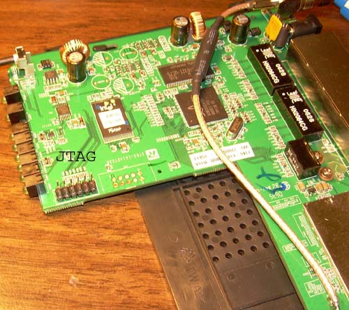
The CPU of the board uses BCM5352. The tool to debug the CPU is EJTAG (DMA).
The JTAG connector is 12 pin, you only need to connect the first 12 pin of 14 pin USB JTAG
| Picture showing JTAG. Some boards are harder to solder pin herders on. You can either remove the solder or directly solder wire on the board |
| Flash | One 2MB | 28F160C3 |
| Firmware | 2MB | $9FC00000-$9FDFFFFF |
| Definition in usbjtag.def | Commands (usbjtag 0.18): |
|
Test: Name=WRT54GS Memory=Ram,0,0x80000000,0x800000 Memory=CFE,1,0x9fc00000,0x40000 Memory=KERNEL,1,0x9fc40000,0x1B0000 Memory=NVRAM,1,0x9fDF0000,0x10000 Programram=0x80200000 Endian=Little IRLength=8 Protocol=EJTAG DMA=Yes ProbTrap=1 |
Backup firmware getram 9fc00000 200000 save 9fc00000 200000 Program whole firmware. (Should not interrupt) detect ldram 9fc00000 program 9fc00000 200000 cmpram 9fc00000 200000 cmpram is optional. It can be used after program only when DMA is supported.After that you should see DEBUG ON. You should see "Compair data OK" |


